Research Overview
Text courtesy of Christie Delfanian, University Marketing and Communications
When it comes to capturing sunlight and converting it into electricity, measuring the physical and chemical properties of thin-film materials is crucial, according to Qiquan Qiao, the Harold C. Hohbach Endowed Professor in Electrical Engineering.
“When we make materials using nanoparticles, nanorods or nanotubes, we need see how such nanostructures are deposited on the substrate,” he said. These nanostructures of optimized dimensions can better trap and absorb sunlight with a wider spectrum, transport and collect the charges more efficiently, thereby increasing solar cell efficiency by capturing and converting more solar energy.
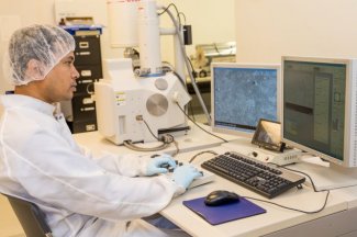
As the director of the Center for Advanced Photovoltaics and Sustainable Energy based in Daktronics Engineering Hall, Qiao oversees three atomic force microscopes and a scanning electronic microscope in Daktronics Engineering Hall.
Qiao and his group are developing new solar cell materials and to increase the efficiency of solar cells. The researchers are improving battery technologies by developing materials that last longer and can store more energy. Seven doctoral students and two master’s students work on this research.
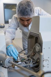
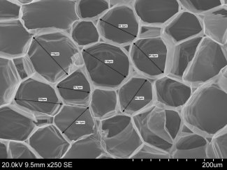
The scanning electron microscope (SEM) uses a focused electron beam which interacts with the atoms in a sample in a vacuum chamber.
“The electron gun injects electrons on the surface. These primary electrons go into the material and kick electrons out of the sample,” Qiao said. A detector collects data on the backscattered electrons based on chemical composition. The stored values are then processed via software to produce a 3D image of the surface structure.
Qiao and his group can track the formation of perovskite nanorods in thin-film materials using the SEM, which is capable of up to 300,000 times magnification.
In addition to characterizing thin-film materials, the SEM provides nanoscale images of biological samples, such as bones and sunflower stems. However, because SEM imaging takes place in a vacuum, biological samples, such as bones and sunflower stems, must be coated with a conductive material, such as gold or silver, explained Assistant Mechanical Engineering Professor Anamika Prasad. “It takes more time, but what we get in return is a finer resolution image.”
The SEM is also suitable for determining the morphology of materials for pharmaceutical and dairy science applications. This provides details about the shape and structure of the material, including the size and positioning of nanoparticles.
Through a two-year, nearly $60,000 grant from the South Dakota Board of Regents, Qiao and his team will increase the resolution of the SEM from 100 nanometers to 10 nanometers by adding field emission scanning capabilities to the microscope.
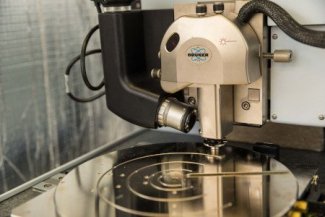
The atomic force microscopes measure the interaction of a probe with the specimen surface. A tiny atomic-scale tip runs across the sample detecting the force between the tip and the surface using a laser.
“It’s a tactile measurement that is very sensitive,” Qiao said. While optical microscopes have a defraction limit, the atomic force microscope can map features on the material surface with subnanometer resolution. That data is then processed to produce a nanoscale image of the specimen surface.
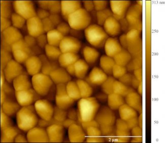
Atomic force microscopy enables researchers developing solar cells, batteries and sensors to determine the morphology of their devices, according to Qiao.
For instance, solar cells developed using perovskite as a semiconductor have achieved high efficiency rates, with a solar panel converting as much as 20 percent of the sunlight into electricity.
“We know the material structure, but we don’t know how it functions to give high efficiency,” Qiao said. The atomic force microscope can help researchers understand the relationship between the material design and the final device performance.
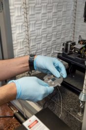
The Bruker atomic force microscope can be used to examine biological samples as well as engineering materials. Assistant Professor Rouzbeh Ghabchi of the Department of Civil and Environmental Engineering is using this microscope to map the nanostructure of asphalt binder.
Through a National Science Foundation-funded project, Qiao and his team developed the capability to do nanoscale mapping of specimens by adding Kelvin probe force microscopy to an atomic force microscope.
This unique Kelvin probe feature allows researchers to map the electrostatic potential of a sample surface, thereby determining the potential charges trapped on the cross-section surface and near-surface region. The data is processed to determine charge carrier lifetime, transport lifetime and diffusion length.
When developing new battery technologies, this capability helps researchers understand why certain nanostructures have a high capacity to store charge, Qiao explained. Furthermore, his research team can study the material’s evolution through multiple cycles.
“We can see why the battery dies after a specific number of cycles,” he said. “We want the material to remain stable. If the anode material degrades and becomes powdery, then the electrode loses its morphology.” Due to this deterioration, the battery loses its ability to hold a charge.
Using this feature, Qiao and his team can also examine the junction between the two semiconductor materials that make up a solar cell. The two semiconductors are comprised of a donor material that absorbs sunlight and excites electrons to produce electricity and an acceptor material that captures the energy. Each donor-acceptor unit absorbs light within a specific wavelength or wave band.
Multijunction solar cells use multiple donor-acceptor layers tuned to different wavelengths gather a greater percentage of the available light energy. The more efficiently the energy moves through these junctions, the better the solar cells perform.
Through these high-power microscopes, researchers can develop thin-film materials that more efficiently capture and store energy.